
Introduciton
This page describes hardware for digital USB DAB transmitter. If u are looking for modulator which utilizes less CPU cycles, take a look at EasyDABv1-USB and EasyDABv2-Ethernet modulators, which is using FPGA for signal processing.
- Nominal Transmit Frequency: 3 ... 206 Mhz (with current PLL loop filter).
- Maximal Tramsmit Frequency: 400 MHz (with 1Ghz reference clock).
- Transmit Power: -60 ... 5 dBm.
- Drivers Installation Needed: Yes
- Software Needed: CRC-mmbtools (multiplexer + modulator)
- LEDs That shows state: Yes (underflow, PLL-lock)
- I/Q samples width: 16 bit
- Complex sample rate: 2048 kS/s.
- External power needed: No
Hardware Description

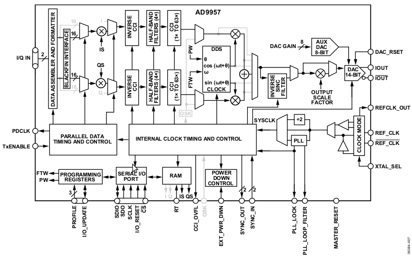
This is the block diagram, that illustrates transmitter design. The AD9957 chip contains 1GSPS DAC this allows to produce signal up to 400 MHz. In current configuration the maximum transmission frequency - is 206 MHz. The FX2 hardware getting 16bit I/Q samples from USB BULK transfers and sending them to AD9957 chip, where it digitally upconverted to specified frequency. The maximal bandwidth of baseband signal for current registers configuration - is 2,048Mhz. Device can be used not only for DAB-transmission, but for DRM+/FM/DVB or other modulation too.
The AD9957 in quadrature upconverter mode:
.png)
The half-band filters (4x) and interpolators (63x) are enabled, this allows to configure PDCLK clock rate to 516096/(2x63) = 4096 KHz (it's for I/Q samples).
The Quartz crystal used in AD9957 schematic - is 24,576 MHz. This quartz is choosed to lock internal PLL for system clock rate to: 24576 * 21 = 516096 KHz.
Schematic and PCB
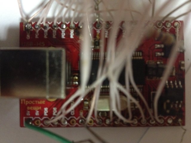
Here is sample of FX2 board: http://oscar.dcarr.org/ssrp/hardware/usb/usb.php
This board is configured to use single endpoint (EP2) in 1024 Bytes mode with 4x buffering (NOTE: sometimes it's not enough for HI-Speed USB transferring). So you must monitor level in TxENABLE pin (it must be always low in normal transfer mode), if it have "1" sometimes - then try to change PC (with better performance), or remove other USB-devices, or in worst case - you need to add fifo buffer between boards (see TODO).
My FX2 board looks like this:
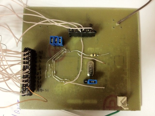
2). The AD9957 prototype board looks like this:
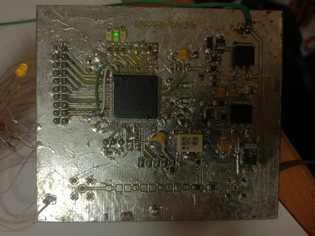
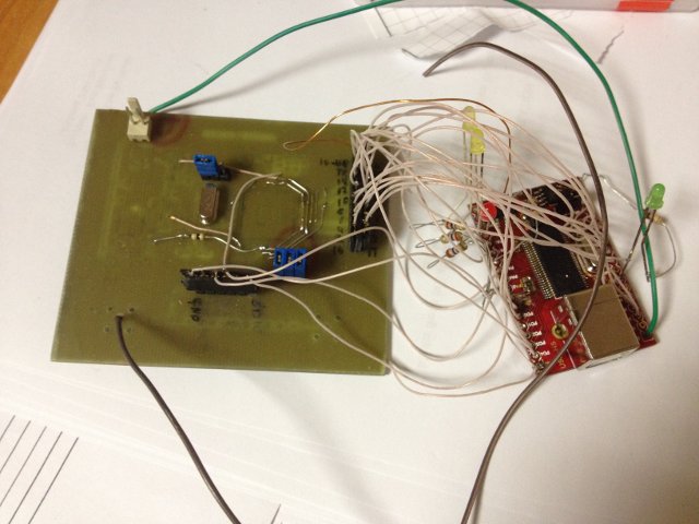
Connected boards:
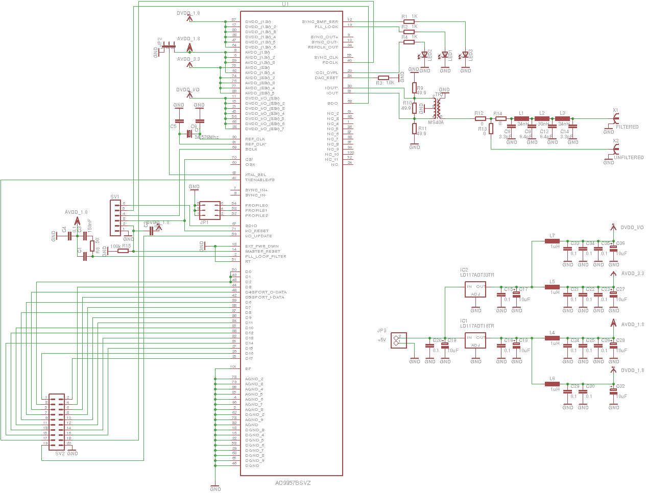
AD9957 Board's schematic (corrected):
Interconnection between FX2 and AD9957 boards:
|
SOFTWARE AND OTHER FILES:
Eagle project for AD9957 test board only: ad9957board.zip (schematic - is ok, but on pcb - there is few conductor are not routed).
Firmware and stand-alone sampling-player software: sdr-dac3.tar.gz (this firmware based on SSRP project).
ChangeLog:
- Control and Data interfaces are splitted in firmware now (this needs for gnuradio).
GNURadio module: gr-ssrptx.tar.gz (github repo: gr-ssrptx). This block is tested and works fine with multiple-stations FM-transmission simulation, dscribed at opendigitalradio page. As additional parameters to GNURadio block you can set:
- Output frequency in hertz.
- Amplitude scale factor [0.0 ... 2.0]
The input format of samples is "sc16" - short complex 16, with fixed samplerate of 2048 kS/s.
Video demonstration:
TODO:
- Enable PDCLK only if we have properly aligned buffer.
- Add FIFO between boards. Due sometimes internal 4Kb buffer is not enough, especially on laptops.
Add GNURadio sink module.(done)- Replace FX2 board by
ATSAM3U or LPC1800AVnet's Xilinx Spartan-6 FPGA LX9 MicroBoard (89$) - Move crc-dabmod modulation algo into FPGA using simulink/system generator.
- Use Microboard's ethernet interface as ETI-receiver and web-interface for DAB transmitter configuration.
- Try to implement DVB-T/T2 transmission.
Board with both chips:
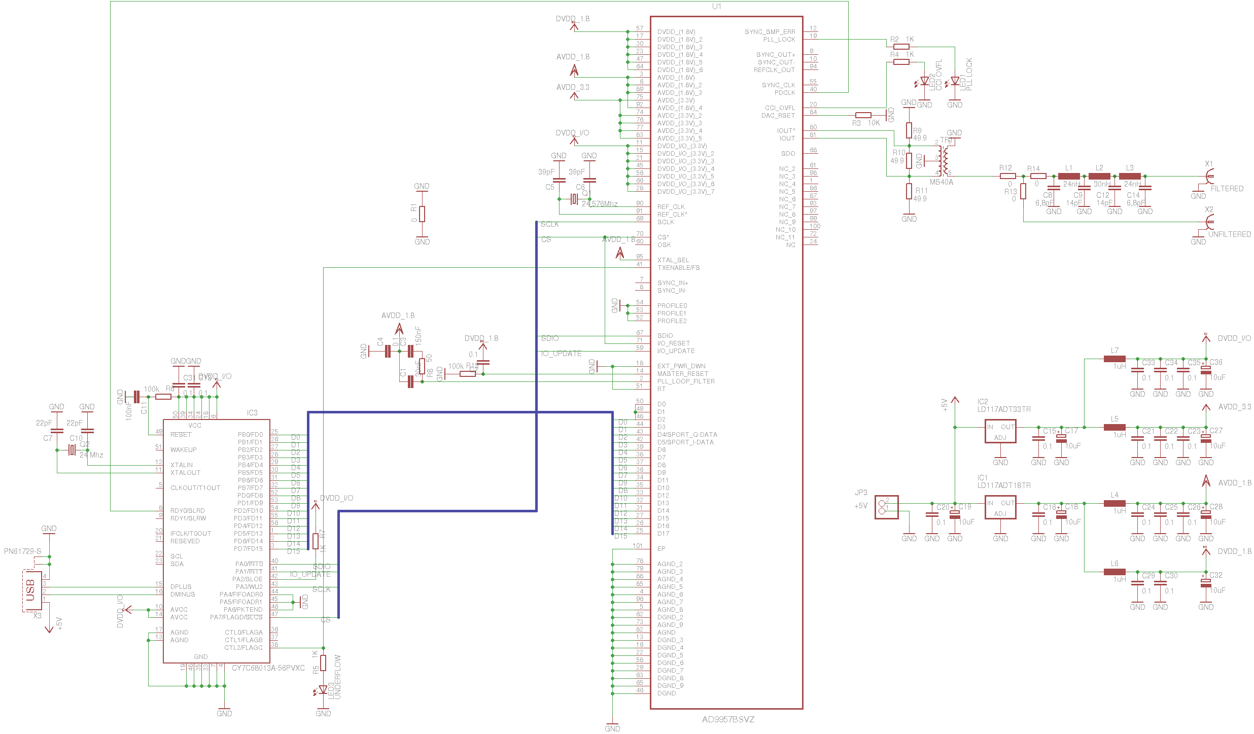
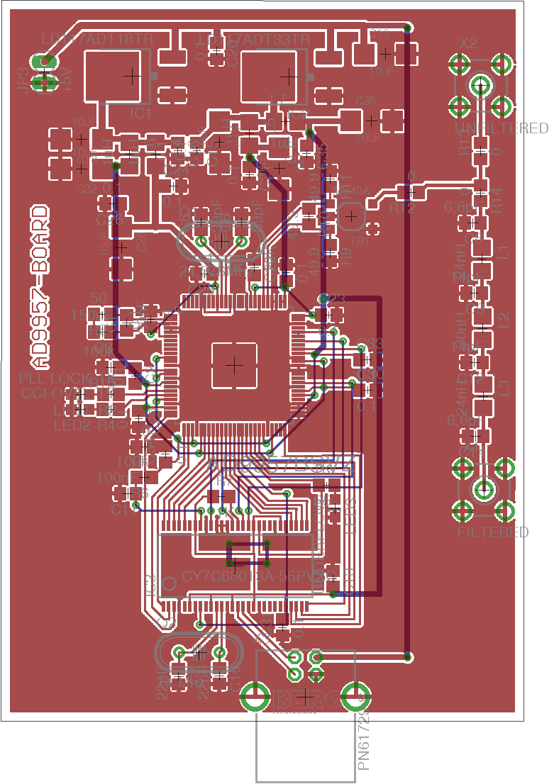
Eagle project ad9957board.tar.gz (NOTE: this pcb is not tested in real-world).
KNOWN PROBLEMS:
- 4096 bytes fifo may be not enough for 2048 kS/s in 16bit mode on slow PC's.
- Sometimes (once from 20 tries) I/Q samples may be swapped due PDCLK may strobes when fc2 mcu not yet set data pins. This is cost of design simplification. The result that you'll have - is inversed spectrum.